                            PRINTED CIRCUIT BOARDS

I have been producing PCB's for my projects for a number of years and I have
found a number of "interesting" methods suitable for building many of my QRP
projects. As always, my methods are very cost conscious (ie. cheap!!).

LAYOUT

The layout of a PCB can be very important so I always lay the components out
as they are in the circuit diagram to begin with. Instead of circuit symbols
I draw the component pins. The drawing is made with a pencil on 1/4" squared
paper.  The compnents are then "shuffled around" with a pencil/eraser to get
a compact layout. Each square of the paper represents 0.1" so resistor leads
are spaced 4 squares appart for horizontal mounting or one square if mounted
vertically. Draw lines between tracks and try various compinations that dont
require tracks crossing. The drawing should be viewed from the top component
side of the board.

1-OFF PCBs METHOD 1 (best looking method)

For complex PCBs you can do quite a lot with a "DALO" or other "etch-resist"
pens.  The hardest part is to accurately position the components so that the
final board looks reasonable. This is how I do it:

With a 0.1" matrix stripboard (veroboard etc.), insert the components in the
positions decided.   At this point you may need to move the odd component to
take into account components with wide bodies etc. Update the pencil drawing
as this will become the component "overlay".

Remove each component and mark the holes in the stripboard with an eraseable
felt-tip marker.  Clamp the stripboard over the copperclad board and a sheet
of flat wood to form a sandwich with the copper clad board in the middle and
the copper side DOWN.   Drill through all the holes marked with the felt tip
pen, and the copper-clad board will be drilled with perfectly regemented 1mm
holes for your components. On the copper side of the copper-clad board, join
the dots with a DALO or other etch-resist pen.  Clean off the stripboard and
re-use it for the next project. The PCB is etched in the normal way.

1-OFF PCBs METHOD 2 (easiest method)

RF PCBs can be made very simply when they are to be used for VHF Power Amp's
up to 10 watts or so.  These boards nearly always have square or rectangular
pads for the RF conductors.   Measure and mark the copper where you want the
track to be and stick SELLOTAPE (UK), DUREX (Australia) SCOTCH TAPE (rest of
the world) where you want the copper to be.   Make certain that there are no
air-bubbles under the tape. Using a sharp knife (or scalpel) and ruler,  cut
around the tracks and remove unwanted tape. This will leave you with tape on
the copper in the positions you want the tracks.  Use a DALO pen if you need
to add the odd thin track. Etch the PCB as usual.

1-OFF PCBs METHOD 3 (fastest method)

Put the copper-clad board in the oven, pre-heated to 120 degrees Celcius and
drop a small lump of candle wax in the centre. Remove the board and allow it
to cool whilst keeping it horizontal. The wax is a good etch-resist, so just
scrape away the wax where you do NOT want the copper to be. A flat modelling
chizel-knife (Xacto etc) is ideal for this. You can use a ruler and felt-tip
pen on the wax without damaging the wax surface. Etch the PCB as usual.

REPEATING PCBs (photo-etch)

This method is a little more "complicated", but I do NOT believe in spending
load of money on UV-exposure boxes etc. A simple 18watt DAYLIGHT flourescent
tube works just as well. This means that you can use photoetch with a simple
working-man's pocket.

Coating the board

Spray the copper side of your board with a "photo-POSITIVE" etch resist in a
dimly-lit dust-free room. Photo-resist is available from:

   Sweden         ELFA and FARNELL
   England        MAPLIN, RS, CirKit and FARNELL
   Middle East    ARAB ENGINEERS (Muhandisoon Al-Arab) and MEJDAF
   USA            RADIO SHACK and TANDY

Making the artwork

Whilst the board is drying, make your artwork. The artwork can be drawn:

a. On drafting film using drafting pens.
b. On a computer drawing program (such as PAINTBRUSH).
c. Using a CAD software package with auto-routing, multilayer capabilities
   and output to a professional quality plotter.
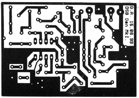
I use methods "a" and "b" (mainly because I am not a millionaire - yet). The
figure above contains a PAINTBRUSH pattern with the correct component
spacing for ICs and standard pads for resistors. The little single dots give
you markers on a 0.1" matrix for planting pads using cut'n-paste.  Print the
finished file reduced to 24%, on tracing paper (ink-jet printer) or OHP film
(Laser printer).   Draw the artwork so that your view of the is from the top
(component side) of the PCB.

Exposure

Expose the PCB in a custom made printing frame. Build up a sandwich of (top
to botom) glass, artwork, copper-clad board and a bit of chip-board (wood).
The artwork must be inky-side down. The copper-clad board must be sensitive
side up. Expose for 2 HOURS 10cm from an 18 watt flourescent tube. You will
have a even and uniform exposure if you  position the tube over one side of
the board for 1 hour, then the other side for the other hour.

Developing

I use one cup of Caustic Soda crystals, dissolved in two cups of water as a
STOCK developer solution.   Use 1ml of this to each 60ml of water to make a
working strength developer. Immerse the board in working strength developer
and the exposed coating will dissolve in seconds.  Wash the board very well
as small traces of soda can contaminate your etchant.

* WHEN MIXING STOCK SOLUTION OF DEVELOPER, MUCH HEAT IS GENERATED. ADD SODA
  VERY SLOWLY AND A SMALL AMOUNT AT A TIME.

ETCHING

Place the board with resist in a vertical tank filled with etchant solution
(normally 1/2 Kg Ferric Chloride to 1 liter of water).  The board should be
totally emersed and vertical.  This will ensure that bubbles are allowed to
rise and the sedement is allowed to fall. I usually support my boards using
plastic clothes pegs (clothes pins). My etching tank is a stout plastic bag
in a wooden former.  The front of my tank is replaced with perspex sheet so
that I can see the board etching. Etching is complete when all the unwanted
copper is dissolved. Wash the board thoroughly after etching is complete.

When you first put the board in the tank the copper will turn a dark colour
where it is exposed.  If bits of WANTED copper turn dark then the board may
be removed, washed and touched up with a DALO pen. If UNWANTED copper stays
nice and shiny then the board may be removed, washed, and carefully scraped
free of the grease or resist that is where it should not be.

The board will normally etch within 15 minutes, less if the etchant is warm
during etching.   Save etchant for re-use on the next PC board in a tightly
stoppered bottle.  When the etchant is almost exhausted the etching time is
increased. If etching takes longer than two hours then adding a little salt
to the etchant will speed it up a little.

AND FINALLY (a word of warning - take this seriously)

Ferric Chloride etchant will stain clothes, carpets, sinks, skin, the wife,
the children and the cat.   It is also poisonous and kills 99% of household
plants.   !!!  FERRIC CHLORIDE CAN SERIOUSLY DAMAGE YOUR MARRIAGE  !!!
Frank, G3YCC